webTV

Lecture

Lancement de la Chaire industrielle ANR TOPAZE

Lecture

Je découvre l'événement "BATMAN" sur Fortnite ! (Pack Batman + Gotham City)

Lecture

Bio-based aerogels: new eco-friendly porous materials for thermal insulation and controlled release

Lecture

LE PIMENT LE PLUS FORT DU MONDE - 10? SI TU REUSSI - Micro Trottoir

Lecture

La chaire industrielle ANR DIGIMU

+ Toutes les vidéos


Scanning Electron Microscopy (SEM)


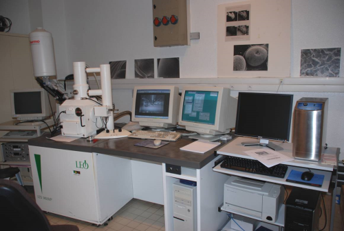
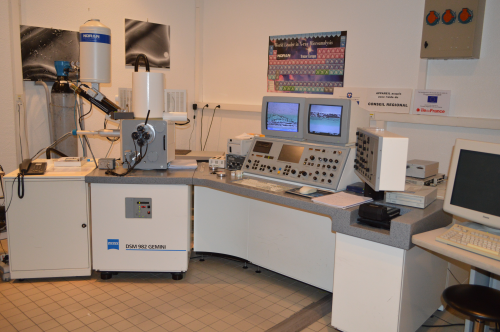
The Centre des Matériaux of the École des Mines de Paris has a long history in Scanning Electron Microscopy (SEM), which began in 1967 with the arrival of the second MEB installed in France ― it was then a SEM Cambridge Stereoscan Mk II equipped with a horizontal and semi-focusing WDS spectrometer with a resolution of 25 nm.

Since then, scanning electron microscopy has evolved considerably and has undergone numerous extensions. Now, in addition to the primary function of making surface images of small-scale samples with different types of detectors, accessories such as X-ray microanalysis (EDS or WDS), diffraction-detecting crystallographic analysis backscattered electrons (EBSDs) have become grafted. Experimental setups have also been adapted to perform in-situ experiments directly in the SEM.

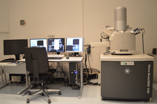
Currently, Maria Betbeder, Lynh-Thy Tran-Hoang and Fabrice Gaslain of the AMI support team, manage the 4 devices available at the Centre des Matériaux. It consists of three SEM (LEO 1450VP, FEI Nova NanoSEM 450, ZEISS DSM982) and a Castaing microprobe (CAMECA SX100).

All of the research teams of the Centre des Matériaux can access these devices and benefit from the expertise of the personnel in charge of scanning electron microscopes. This fleet of instruments and the know-how of the team can be solicited as part of valuation studies through VAL Tech.

__________________________________________________________________________________________


__________________________________________________________________________________________

SEM LEO 1450VP

Main features
  • Installation : 2000
  • 30 kV, barrel equipped with a tungsten filament (W)
  • Variable pressuree
  • Nominal resolution : 3.5 nm to 30 kV
  • Useful magnfications : from 20 to 80 000 x
Detectors, accessories and specificities
  • Large room, motorized stage (5 axes) with high deflections.
  • Low vacuum for observing non-conductive samples.
  • Detectors :
    • SE in the chamber (Everhart-Thornley) ;
    • VPSE detector (Low Vacuum) ;
    • Retractable BSE with 4 quadrants.
EDS X microanalysis system

Thermo-Noran's Si (Li) "System 6" microanalysis system with the following characteristics :
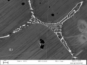
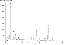
  • Energy resolution of 131 eV @ Mn Kα at 1500 cps.
  • Detection of elements possible from the element boron.
  • Opportunities to perform many tasks :
    • EDS acquisition with qualitative, semi-quantitative and quantitative analysis (with or without controls) of the spectra obtained ;
    • Acquisition of SEM images followed by acquisition / multipoint analysis EDS ;
    • Acquisition and analysis of qualitative line profiles ;
    • Acquisition and analysis of X qualitative, quantitative and phase analysis mappings.

(1) Matrice

(2) Carbonitrure

(3) Borure

__________________________________________________________________________________________

SEM FEI Nova NanoSEM 450

Main features
  • Installation : 2012
  • 50 V to 30 kV, S-FEG gun equipped with a Shottky point
  • Indicative probe current : 0.6 pA at 200 nA
  • High resolution column with sufficient current to quickly perform EDS mapping and low and high magnification EBSD analyzes
  • Resolutions : 1 nm to 15 kV, 1.4 nm to 1 kV, 3 nm to 15 kV / 5 nA / WD 5 mm
  • Useful magnifications : from 35 to 600 000 x
Detectors, accessories and specificities
  • Large chamber, motorized stage (5 axes) with high deflections.
  • Low vacuum for observing non-conductive samples.
  • Detectors :
    • SE,
    • Retractable BSE (CBS) large area with cut-off voltage at +1000 V,
    • SE In-Lens and BSE In-Lens (TLD),,
    • SSE Low Vacuum and specific BSE (GAD) with an X-ray cone equipped with a differential diaphragm of 500 μm thus limiting the pressure with the final lens.
  • Polarized plate from +50 V to -4000 V.
  • Current measurement from 1 pA to 2 μA.
  • Software allowing automatic multi-field acquisition.
  • Software dedicated to electronic lithography for the engraving of complex patterns.
  • Automation : possibility to work on large areas or work at night.
EDS X microanalysis system

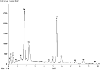
Bruker XFlash 5030 127 eV EDS SDD energy selection microanalysis system with Quantax 800 software suite with the following features :

  • Energy resolution of 127 eV @ Mn Kα (54 eV @ C Kα, 64 eV @ F Kα), guaranteed up to 50,000 cps.
  • Detection of elements possible from the element boron.
  • Opportunities to perform many tasks :
    • EDS acquisition with qualitative, semi-quantitative and quantitative analysis (with or without controls) of the spectra obtained ;
    • Acquisition of SEM images followed by acquisition / multipoint analysis EDS ;
    • Acquisition and analysis of qualitative and quantitative line profiles ;
    • Acquisition and analysis of qualitative and quantitative spectral X-ray mappings (in single or multi-fields) ;
    • Acquisition and morpho-chemical analysis of particles or inclusions (mono or multi-field).
EBSD system

EBSD rapid acquisition system of crystallographic orientation cartographies EDAX OIM Hikari.

  • IOM Suite v6.1 for complete data acquisition and processing.
  • Fast camera with a CCD 640x480 pixel resolution allowing a maximum acquisition / indexing speed of 320 img / sec (binning 10x10).
  • Single or multi-field acquisition.
  • Possibility to work indifferently on massive samples or thin lamellas (mode of reflection or transmission).
Traction plate

Micro-platinum traction / compression equipped with 2 force cells (100 N and 5000 N) with a displacement of 10 mm.


__________________________________________________________________________________________

SEM ZEISS DSM982 Gemini

Main features
  • Installation : 1994
  • from 500 V to 30 kV, FEG gun equipped with a Schottky point
  • Gemini High Resolution Column
  • Nominal resolution: 1 nm to 20 kV, 4 nm to 1 kV
  • Useful magnifications : from 50 to 200 000 x
Detectors, accessories and specificities
  • Large chamber, motorized stage (4 axes) with high deflections
  • Detectors :
    • SE in the chamber (Everhart-Thornley),
    • SE In-Lens,
    • Retractable BSE with 4 quadrants,
    • CI (current absorbed),
    • TE (transmitted electrons - dark background).
  • Current measurement from 1 pA to 2 μA
EDS X microanalysis system

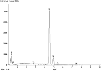
Si (Li) energy-selective X-ray microanalysis system at Noran Voyager IV station with the following characteristics :

  • Energy resolution of 131 eV @ Mn Kα at 1500 cps.
  • Detection of elements possible from the element boron.
  • Opportunities to perform many tasks :
    • EDS acquisition with qualitative, semi-quantitative and quantitative analysis (with or without controls) of the spectra obtained ;
    • Acquisition and analysis of qualitative line profiles ;
    • Acquisition and analysis of qualitative X ROI mappings.
EBSD  system

Nordif UF300 rapid acquisition system EBSD for rapid acquisition of crystallographic orientation maps.

  • Acquisition with Nordif UF software.
  • IOM suite v6.1 for full indexing and data processing.
  • Fast camera with a CCD 640x480 pixel resolution allowing a maximum acquisition / indexing speed of 300 img / sec (binning 10x10).
  • Possibility of working indifferently on massive samples or thin lamellas.


__________________________________________________________________________________________

Castaing microprobe CAMECA SX100

Main features
  • Installation : 2008
  • 4 wavelength dispersion spectrometers : 12 analyzer crystals (1 PC1, 1 PC2, 1 LPC2, 3 TAP, 2 LiF, 1 LLiF, 2 PET, 1 LPET)
  • 1 Bruker AXS 1100 SDD energy selection spectrometer
  • Optical field camera from 262 μm to 1600 μm
  • Sample plates that can support up to 6 polished flat samples of Ø 25 mm and 17 mm thickness.


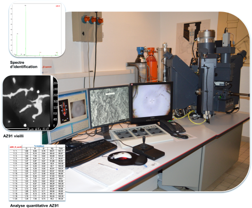
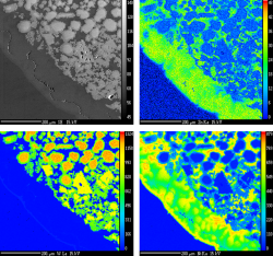
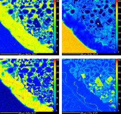
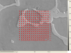
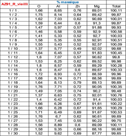
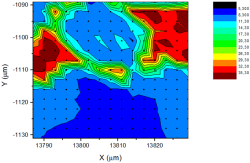
The Castaing Cameca SX100 microprobe can be used to perform quantitative X-scale microanalysis and X-ray mapping.
This unit is equipped with a liquid nitrogen trap and an oxygen leak to limit carbon contamination on the samples. The motorization of the sample plate allows the launch of numerous automatic quantitative analyzes and X-images on 6 polished flat samples.

Cartography X - WC depot on a steel


Field of activity

  • Observation and acquisition of SEM images (SE, BSE and absorbed current)
  • Precise and non-destructive chemical analysis in a volume of the order of μm3 with a sensitivity of ~ 100 ppm and a precision of ~ 1%
  • Qualitative, semi-quantitative and quantitative analysis of chemical elements ranging from boron to uranium
  • Realization of X maps to observe the distribution of elements
  • Measurement of thicknesses and compositions of thin layers
  • Analysis of all types of materials requiring precise knowledge of the local chemical composition : metals, composites, polymers, glasses, ceramics, etc.

__________________________________________________________________________________________


Scanning Electron Microscopy (SEM) - MINES ParisTech
Partager

news

A new version of the  COLD SPRAY CLUB website is now online!

A new version of the COLD SPRAY CLUB website is now… The COLD SPRAY CLUB concerns laboratories, technology…
> En savoir +

A MINES ParisTech PhD student awarded at the International Symposium on « High-Temperature Corrosion and Protection of Materials »

Formation A MINES ParisTech PhD student awarded at the… Josiane Nguejio, PhD student at Centre des Matériaux…
> En savoir +

The FEMS Lecturers 2014-2015 include Henry PROUDHON

Recherche The FEMS Lecturers 2014-2015 include Henry PROUDHON Lecturer Series This is a scheme which sponsors selected…
> En savoir +

award for a team of Centre des Matériaux

Recherche award for a team of Centre des Matériaux Nicolas Gueninchault who work in teams M2 and COCAS with Henry…
> En savoir +

Recherche The SF2M award three medals to doctors of the centre des… The medal Réaumur is given by  SF2M, each two…
> En savoir +

+ More articles

calendar

+ More events

Plan du site
Mentions légales efil.fr © 2014 MINES ParisTech